Final test results of the CAN LMB and components after the irradiation

Date of  test before radiation 7/4  and 16/4 1998. The first irradiation period 29/4 to 13/5 1998,  the second irradiation period 17/6 to 8/7 1998 and the third period of test  5/8 to 21/9 1998

Dose rate of the period 1 (14 days) was   26Gy  (±25%) and neutrons (equiv. 1 MeV Si) was  2 1011 neutrons cm-2  (±50% )
Dose rate of the period 2 (20 days) was   48 Gy  (±25%) and neutrons (equiv. 1MeV Si) was  5 1011 neutrons cm-2  (±50% )
Dose rate of the period 3 (45 days) was  140Gy  (±25%)and neutrons (equiv. 1MeV Si) was  1.1 1012 neutrons cm-2  (±50% ).
Total dose rate for a period of  79 days  was  214 Gy  (±25%) and neutrons (equiv. 1MeV Si) was  1.8 1012 neutrons cm-2 (±50% )
 
For a general description of the tests and the test  area TCC2,  see  radtests.html

Below the detailed results are  presented:


PCA82C250
Component:  Philips CAN-bus controller interface circuit PCA82C250, RS components 189-2254. The circuit is the interface between the CAN protocol controller and the physical bus. The provides differential transmit capability to the bus and the differential receive capability to the CAN controller. It is used in the package SMD SOIC-8. The circuit is mounted on an adapter SOIC-8 to DIL-8 from Winslow W9501 RS components 160-5432.

Philips lot-number: 64HAI   J054Y

Description: Four circuits were tested in the test-box circuit. See Appendix 1

Test results:


Table : 1 Measured pulse period in the test circuit.
Component PCA82C250 Pulse Period (ns) (before irradiation)  Period (ns) after  1:st irrad Period (ns) after 2:nd irrad
 Period (3:rd) after irrad
CH027
437
437
439
440
CH026
436
437
444
444
CH025
441
440
441
444
Reference CH024
439
434
439
440
Table 2: Measured pulse width in the test circuit.
Component PCA82C250 Pulse Period (ns) (before irradiation)  Period (ns) after1:st irrad.  Period (ns) after 2:nd
 Period after(3:rd)
CH027
253
255
256
251
CH026
253
255
255
251
CH025
256
256
258
256
Reference CH024
252
252
255
252
Table 3: Measured current consumption of the PCA 82C250 in the test circuit.
Component PCA82C250 Pulse Period (ns) (before irradiation)  Period (ns) 1:st Period (ns) 2:nd
 Period (3:rd)
CH027
49.22
49.09
49.48
48.90
CH026
48.01
48.10
49.01
48.33
CH025
49.36
50.32
49.31
49.44
Reference CH024
49.43
48.71
49.26
48.90
Comments:  The circuit is tested at twice the maximum speed as used in the CANbus application. One reference circuit was selected and is not tested in radiation.
Conclusions: There is no significant influence of the radiation.

IL206A
Component: Siemens Optocoupler IL206A (RS components 192-5382)  is an optically coupled pair with a Gallium Arsenide infrared LED and a silicon NPN phototransisitor. It is used in the package SMD SOIC-8. The circuit is mounted on adapter SOIC-8 to DIL-8 Winslow W9501 RS components 160-5432.

Siemens lot number:   9652Y

Description: Six circuits were tested in the test-box circuit. Five of these were then subjected to radiation, while one was kept as reference.


Table 4: Measured pulse period in the test circuit RC=2.2k except after the period 3 where RC was changed to 34.7k.
Component IL206A
Period (us) (before rad)
 After Period 1 (us)
 After Period 2
 After Period 3
CH023
15.561
15.015
 does not work
36.5
CH022 (reference)
15.488
15.699
 15.532
57.1!
CH021
15.573
15.084
 does not work
 37.0
CH020
15.715
15.101
 does not work
 37.0
CH019
15.477
14.975
 28.386
 34.8
CH018
15.483
15.296
does not work 
 40.4
Table 5: Measured pulse width.
Component IL206A
Period (us) (before rad)
 Period (us) (after 1:st rad)
 Period (us) (2:nd)
 Period (3:rd)
CH023
3.518
4.451
 does not work
14.9 
CH022 (reference)
3.472
3.512
 3.496
 2.7
CH021
3.613
4.547
 does not work
 15.6
CH020
3.549
4.459
 does not work
 15.5
CH019
3.503
4.298
 8.956
 12.1
CH018
3.710
4.894
 does not work
 20.3
Table 6: Measured DC current consumption for a load of 2.2kohms.
Component IL206A
DC current (mA) (before rad)
 DC current (mA) after 1:st rad)
 Period (2:nd) (mA)
 Period (3:de)
CH023
2.564
2.510
 2.230
 
CH022 (reference)
2.568
2.585
 2.572
 -
CH021
2.557
2.506
 2.252
 -
CH020
2.564
2.506
 2.249
 -
CH019
2.564
2.517
 2.308
 -
CH018
2.549
2.487
 2.057
 -
Table 7: Current Transfer Ratio (a diode current If = 8.3mA, VCE=3.5V).
Component IL206A
Transsitor DC current (mA) (before rad)
 Transistor DC current (mA) 
(after 1:st rad)
 DC current (mA) 
(after 2:nd rad)
 DC current (mA) 
(after 3:rd  rad)
CH023
7.569   CTR=91.2%
5.078   CTR=61.2%
 2.308 CTR=27.8
 0.311 CTR=3.75
CH022 (reference)
7.528   CTR=90.7%
7.491   CTR= 90.3%
 7.472 CTR=90.0
7.473  CTR=90.0
CH021
7.030   CTR=84.7%
4.870   CTR=58.7%
 2.328 CTR=28.0
 0.298 CTR=3.59
CH020
7.613   CTR=91.7%
5.094   CTR=61.4%
 2.322 CTR=28.0
 0.281 CTR=3.39
CH019
7.529   CTR=90.7%
5.262   CTR=63.4%
 2.676 CTR=32.2
 0.352 CTR=4.24
CH018
6.760   CTR=81.4%
4.526    CTR=54.5%
 2.107 CTR=23.7
 0.251 CTR=3.02
The data sheet gives a CTR of  63 to 125 % for If=10mA and VCE=5V.

Comments:     
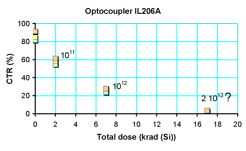
Results from the 1:st irradiation show a reduction of the current transfer ratio of about 70% and there is one device (CH018) which does not fulfill the specifications. The results from the 2:nd rad test show that the current transfer ratios are reduced about 45% during the test. Only one of five optocouplers is still working in the AC test for a RC =2.2k. After period 3 the RC was changed and therefore the optocouplers could be made working.
Conclusions:   The mean value of the current transfer ratio changed from 88 to 3.6%.  With a change of the gain of the circuit (the collector resistance RC was increased from 2.2 kohms to 35 kohm) it was found that the optocouplers were still functional!


ADM660
Component: Analog Devices ADM660 CMOS switched-capacitor charge-pump converter to invert to input supply voltage. It is used in the package SMD SOIC-8. The circuit is mounted on adapter SOIC-8 to DIL-8 Winslow W9501 RS components 160-5432.

Analog Devices  lot number:  9722:

Description: Four circuits were tested in the test-box circuit. One was kept as reference and the other three was irradiated.


Table 8: Output voltage in the test circuit.
Component ADM660 Vout (V) before irradiation  Vout (V) after 1:st rad Vout (V) after 2:nd rad 
 Vout (V) after 3:rd rad
CH017
-5.974
-6.006 (-32mV)
-5.978 (-4mV)
-5.960 (+14mV)
CH016
-5.974
-6.005 (-31mV)
-5.976 (-2mV)
-5.955(+19mV)
CH015
-5.967
-6.006 (-39mV)
-5.973 (-6mV)
-5.947(+20mV)
Reference CH014
-5.970
-6.007 (-37mV)
-5.974 (-4mV)
-5.941(+29mV)
Table 9: Current consumption in the test circuit.
Component ADM660 Current (mA) before irradiation  Current (mA) after 1:st rad Current (mA) after 2:nd rad 
Current (mA) after 3:rd rad
CH017
12.747
12.795
12.746
12.705
CH016
12.703
12.746
12.690
12.636
CH015
12.715
12.767
12.698
12.639
Reference CH014
12.738
12.805
12.751
12.679
Table 10: Noise voltage measured  in the test circuit.
Component ADM660 Noise (mVpkpk) before the rad.  Noise (mVpkpk) after 1:st rad Noise (mVpkpk) after 2:nd rad
Noise (mVpkpk) after 3:rd rad
CH017
212
202
172
178
CH016
212
199
170
175
CH015
209
193
168
175
Reference CH014
222
209
181
201
Comments:  The switching noise is to a large extent due to the test setup.
Conclusions:  There is no noticable effect of the irradiations compared to the reference circuit.


AD680
Component: Analog Devices AD680 bipolar bandgap reference which provides a fixed 2.5V output from inputs between 4.5 V and 36 V.  The JR version with 10 mV initial accuracy. It is used in the package SMD SOIC-8. The circuit is mounted on adapter SOIC-8 to DIL-8 Winslow W9501 RS components 160-5432. The circuit is loaded with 5mA
Analog Devices lot number: JR9640 B39480

Description: Four circuits were tested in the test-box circuit.


 Table 11: The output voltage as measured in the test circuit.
Component AD680
Vout (V) before irradiation  Vout (V) after 1:st rad Vout (V) after 2:nd rad 
 Vout (V) after 3:rd rad
CH010
2.4992
2.4987 (-0.5 mV)
2.4970 (-2.2mV)
2.4956 (-3.6mV)
CH011
2.5039
2.5026 (-1.3 mV).
2.5019 (-2.0mV)
2.5002 (-3.7mV)
CH013
2.4998
2.4995 (-0.3mV)
2.4987 (-1.1mV)
2.4963 (-3.5mV)
Reference CH012
2.5004
2.5005 (+0.1mV)
2.5005 (+0.1mV)
2.5004 (0.0mV)
Table 12: The current consumption is the test circuit was.
Component AD680
Current (mA) before rad.  Current (mA) after 1:st rad Current (mA) after 2:nd rad 
 Current (mA) after 3:rd rad
CH010
5.061
5.062
5.078
5.050
CH011
5.068
5.066
5.077
5.058
CH013
5.064
5.065
5.073
5.053
Reference CH012
5.064
5.066
5.080
5.065
Table 13: The noise measured in the test circuit.
Component AD680
Noise (uVrms)  before irradiation  Noise (uVrms)after 1:st rad Noise (uVrms)  after 2:nd rad 
 Noise (uVrms)  after 3:rd rad
CH010
911
736
609
990
CH011
924
682
588
1013
CH013
870
775
586
1001
Reference CH012
890
725
604
980
Comments:    The noise is dominated by external pickup!
Conclusions: There is a small decrease of the output voltage of -3.6mV, which is still within the specifications.


ADP3301
Component:  Analog Devices ADP3301 high Accuracy anyCAP 100 mA low dropout linear regulator voltage reference. it has 0.8% initial accuracy.   It is used in the package SMD SOIC-8. The circuit is mounted on adapter SOIC-8 to DIL-8 Winslow W9501 RS components 160-5432.

Analog Devices lot number:  AD 739 3301A 5

Description: Four circuits were tested in the test-box circuit. The circuit is loaded with 48mA.


Table 14: The output voltage as measured in the test circuit.
Component ADP3301 Vout (V) before irradiation  Vout (V) after 1:st rad Vout (V) after 2:nd rad 
 Vout (V) after 3:rd rad
CH006
4.993
4.994 (+1 mV)
4.998 (+5mV)
4.999 (+4mV)
CH007
5.005
5.005 (0 mV).
5.005 (0mV)
5.010  (+5mV)
CH009
4.994
4.994 (0mV)
4.995 (+1mV)
4.998 (+4mV)
Reference CH008
4.997
5.000 (+3mV)
4.999 (+2mV)
4.999 (+2mV)
Table 15: The current consumption as measured in the test circuit.
Component ADP3301 Current (mA) before irradiation  Current (mA) after 1:st rad Current (mA) after 2:nd rad 
 Vout (V) after 3:rd rad
CH006
48.38
48.38
48.47
48.58
CH007
48.51
48.50
48.56
48.79
CH009
48.43
48.42
48.49
48.72
Reference CH008
48.43
48.43
48.45
48.46
Table 16: The noise voltage in the test circuit.
Component ADP3301 Noise (uVrms) before irradiation  Noise (uVrms) after 1:st rad  Noise (uVrms) after 2:nd rad
 Noise (uVrms) after 3:rd rad
CH006
800
709
600
691
CH007
770
1425 (! sdev normal)
836
570
CH009
778
720
591
677
Reference CH008
833
761
615
668
Comments: The noise is dominated by external pickup!
Conclusions: This circuit is not sensitive for radiation up to the tested levels.

Test results of the LMB CAN node Pt100

The results from measurements of the LMB before and after the 1:st radiaton:

     Table 17: Measured value of one 100 ohms reference resistor.
Date 
22.4 1998 (before) 
23.4 1998 (before)
13.5 1998 (after 1:st irrad) 
14.5 1998 (after 1:st irrad)
LMB Pt100 Mean value (ohms) 
100.003
100.013
100.023
100 .004
LMB Pt100 (rms of 8 channels) (ohms)
0.030
0.039
0.041
0.050
The results show no clear effect of the radiation.

Comments:  After the second irradiation the Pt100 part did not respond probably due to the reduced gain of the optocouplers! With another Pt100 module the response was normal!  After the complete test period the CAN controller is still responding normally, while the ADC part  is not probably due to the optocouplers.


 Test results of the AT90S1200

Five ATMEL AT90S1200 RISC processors with  flash memory and EEPROM data storage were programmed with the same software: RAD98A.ROM and RAD98A.EEP.
The AT90S1200 has 64 bytes of EEPROM and 1024 bytes of flash PROM.

 Table 18: Measured contents of the memories of the processor AT90S1200.
Device  AT90S1200 
23.4 1998 (before)
13.5 1998 (after 1:st) 
 13.7 1998(after 2nd)
2.10 1998 End of test
CH001 
Ok
One error in EEPROM  
address 041C is FFH should be 15H!!
One error in EEPROM  
address 041C is FFH should be 15H!
One error in EEPROM 
address 041C is FFH should be 15H
CH002
Ok
Ok
 One error in EEPROM  
address 0438 is FFH instead of 20H!!
One error in EEPROM 
address 0438 is FFH instead of 20H!
CH003
Ok
Ok
Ok 
Ok
CH004
Ok
Ok
Ok
Ok
For details see the  memory dump  AT90S1200 dump

Conclusions:  There was twice a memory location in the EEPROM area which was erased. However this could be repgrammed and all chips are functional after the complete test. The
EEPROM seems to be more sensitive than flash PROM.


 Updated 6.1 1999 B.Hallgren